The champion of micro surface observation. The first step of a scientific evaluation is to thoroughly observe the form of the material. For this purpose, we have a magnifying glass or an optical microscope. But, as long as light is used, we can’t see anything smaller than the wavelength of light and therefore observing a nano structure is extremely difficult.
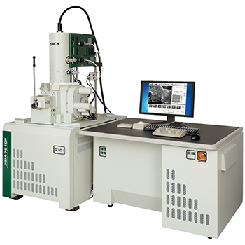
The Scanning Electron Microscope (SEM) introduced here utilizes an electron beam whose wavelength is shorter than that of light and therefore observing a structure down to several nm in scale becomes possible.
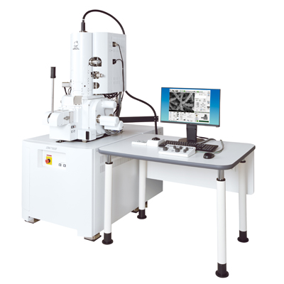
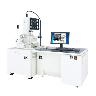
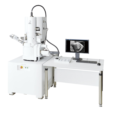
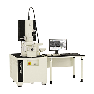
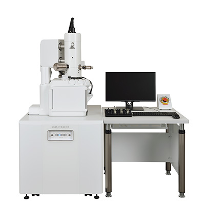
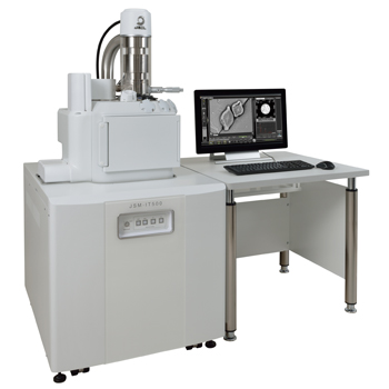
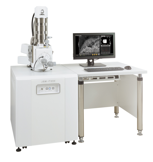
The Scanning Electron Microscope, which is utilized in various fields such as medical, biological, metals, semiconductors and ceramics, is broadening its application frontier. With abundant attachments and devices being combined, its capability is expanding. SEM is regarded as one of the most powerful tools being used at R&D institutes and quality control inspection sites all over the world. JEOL provides a wide variety of scanning electron microscopes for your applications.(Ex: JSM-7900F Schottky Field Emission Scanning Electron Microscope, JCM-7000 NeoScope™ Benchtop SEM,JSM-IT200 InTouchScope™ Scanning Electron Microscope)